Welcome to GaNo Optoelectronics Inc
Key Technology Product Comparison Common Questions
Technology Introduction
Key Technology
       Since ultraviolet (UV) radiation has a strong impact on both organic and inorganic materials, it has extensive applications in the fields of industry, agriculture, medicine and health, and environment monitoring, which gives rise to a huge market of UV sensors and related application products. To meet the urgent demand for high-end UV sensing applications, GaNo Optoelectronics has been developing and producing high-performance UV sensors based on a new generation electronic material – wide bandgap semiconductors.

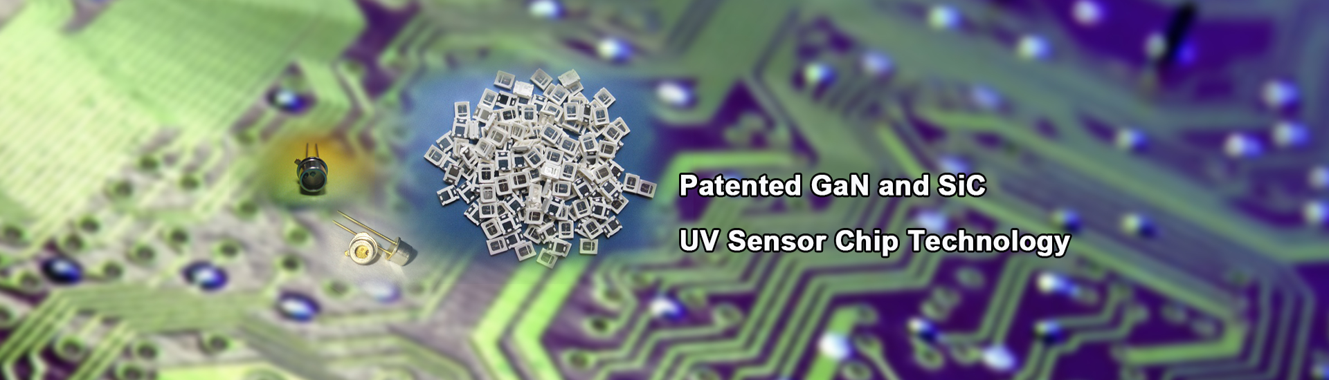
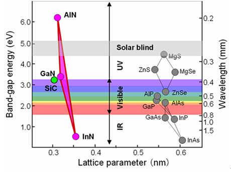
       Currently, based on the bandgap energy of semiconductor materials used, semiconductor UV sensors can be divided into two major categories: one is photodiode made with conventional semiconductor materials (such as Si, GaAs and InP), while the other is photodiode made with wide-bandgap semiconductors (such as GaN and SiC). The former category has already been technically mature. Nevertheless, since the bandgap of the semiconductor used is relatively narrow, the peak response of the corresponding sensors is usually within the visible wavelength region. Therefore, to make these sensors selectively work in UV wavelength region, additional optical filters have to be added, which are specially designed and very expensive. Since the intensity of visible light of solar radiation reaching the ground is over 104 times stronger that of UV light, the aforementioned filter requires a high rejection ratio, and is thus very difficult to manufacture. Besides, while filtering out the high-intensity visible light, the filter would also filter out a considerable amount of UV light to be detected, resulting in a greatly reduced quantum efficiency of the UV sensing system. In comparison, the photodiode technology based on wide-bandgap semiconductors developed by GaNo Optoelectronics can effectively solve the above problem.


       Wide-bandgap semiconductors represented by SiC and group-III nitrides are new generation semiconductor materials and have become the focus of research and development worldwide in recent years. These semiconductors exhibit large bandgap energy, high thermal conductivity, high electron saturation velocity, and excellent chemical stability. Due to these outstanding material properties, wide bandgap semiconductors have key applications for high-frequency, high-power, and high thermal resistant devices as well as high efficiency optical sensing devices working in UV wavelength band. Among them, 4H-SiC semiconductor has a bandgap energy of 3.23 eV and is an ideal material for making visible-blind UV sensors (with a cutoff wavelength<400 nm). On the other hand, by varying Al content, the bandgap energy of AlGaN within group-III nitride system can continuously change from 3.4 to 6.2 eV. The corresponding wavelength range of optical response is 200-365nm, which covers the solar-blind wavelength region (240-280nm) caused by the ozonosphere absorption. Thus, AlGaN is suitable for making new generation solar-blind deep UV sensors (see the following figure). Compared with conventional Si-based UV sensors, the UV sensors based on wide-bandgap semiconductors have the following advantages:
1. higher sensitivity in UV wavelength region;
2. visible blind or solar blind operation without a filter;
3. reliable operation in harsh environment such as high temperature and intense radiation.

Fig. Bandgap energy and cutoff wavelength of main semiconductor materials