GaNo Optoelectronics Inc. is a spin-off high-tech company from Nanjing University, focusing on developing and producing next generation high sensitivity ultraviolet (UV) sensors, application modules, as well as offering technical consulting services related to UV sensing. GaNo Optoelectronics was established in 2013 with its headquarter and R&D center located at Nanopolis Suzhou, China. The core team of GaNo Optoelectronics has strong R&D capability and rich experience in semiconductor device manufacturing. The mission of GaNo Optoelectronics is to develop world-class UV sensing devices, leading to perfect solutions for highly sensitive and accurate UV detection.
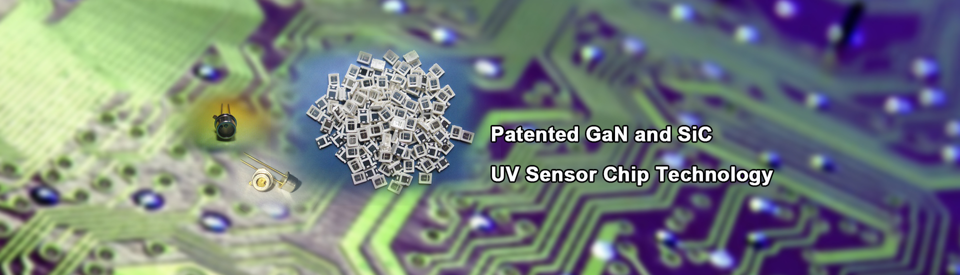
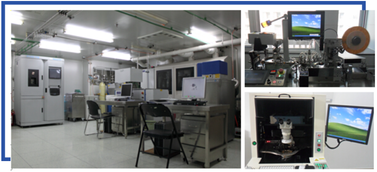
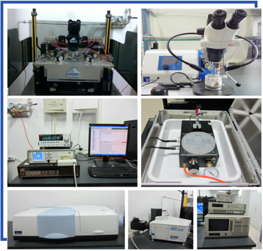
GaNo Optoelectronics is committed to developing and producing high performance UV sensing devices based on wide-bandgap semiconductors, which have drawn world-wide R&D interest in recent years. Wide-bandgap semiconductors, such as GaN and SiC, have many intrinsic material advantages, such as large bandgap energy, high thermal conductivity, high electron saturation velocity and chemical stability, making them suitable to be developed as backbone material for energy-efficient high frequency and high power devices as well as optical sensing devices working specifically in UV band. GaNo Optoelectronics has completed the qualification of a device processing line and a high standard device testing lab. Through these efforts, GaNo Optoelectronics is a leading company in China, which offers mass supply of high performance GaN and SiC UV sensing products with various packaging types.
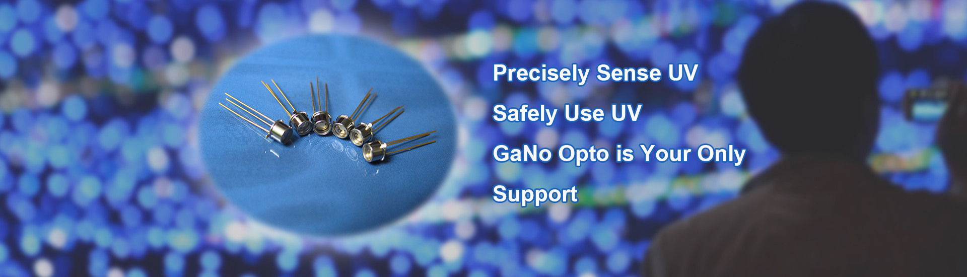
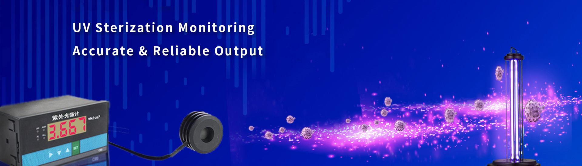
The UV sensors produced by GaNo Optoelectronics have the characteristics of high responsivity, low dark current, and fast response speed, resulting in significantly higher cost performance compared with similar products on the market. These UV sensors have key applications in environmental monitoring, UV curing, chemical/bio-agent detection, food/water/air sterilization, water quality monitoring, and flame detection.
While maintaining technological leadership, GaNo Optoelectronics will establish and implement highly timely and cooperative customer service standard. GaNo Optoelectronics will not only offer high quality UV sensing products, but also offer complete consulting service and solutions for product applications. The long term goal of GaNo Optoelectronics is to become a global leading company in the field of UV sensing and related applications.